Rear I/O
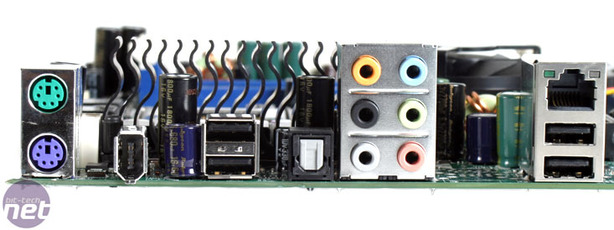
The rear I/O actually looks a little sparse. With the removal of one of the two Gigabit Ethernet sockets this means that the associated USB ports have been moved up the motherboard to keep a complement of four.There is still one RJ45 Gigabit Ethernet socket, two PS2 ports, a 6-pin Firewire port and six 3.5mm analogue audio jacks supplying not only the 8 channel sound, but line in and microphone ports as well. Optical S/PDIF out is provided, with S/PDIF in accessible via motherboard pins, however nothing has been provided to make use of them. There is unfortunately no coaxial S/PDIF at all.
BIOS
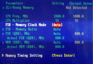
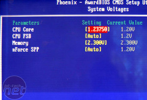
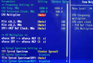
Frequency Adjustments:
PCI-Express x16 slots (100-200MHz in 1MHz increments); SPP-MCP Hyper Transport (200-500MHz in 1MHz increments); HyperTransport multiplier (1-5x); Front Side Bus (QDR - 400-2500MHz in 1MHz increments); Memory (DDR - 400-1400MHz in 1MHz increments);
Voltage Adjustments:
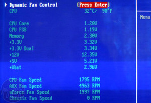
CPU Core (0.8V to 1.6V in 0.00325V increments); CPU FSB (1.2V to 1.4V in 0.1V increments); Memory (1.8V to 2.5V in 0.025V increments); Northbridge (1.5V to 1.7V in 0.025V increments); Southbridge (1.5V to 1.75V in 0.25V increments); HyperTransport (1.2V to 1.55V in 0.05V increments);
Memory Timings:
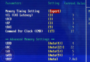
CAS Latency (tCL), RAS to CAS Delay tRCD, RAS to CAS Delay tRP, RAS Cycle Time (tRAS), Command Rate, Row Active to Row Active Delay (tRRD), Row Cycle Time (tRC), Write to Read Time (tWR), Internal Write to Read Command Delay (tWTR), Time between RAM refreshes (tREF).
The memory timings are not overly comprehensive to complicate matters, but still the essential adjustments plus a few extra are supplied. While digital PWMs would give you greater and finer voltage adjustments, what's necessary is included. The overvoltage adjustments have been cut down from the full fat nForce 680i SLI though: CPU voltage limit has been reduced from liberal 1.8V to a tame 1.6V, northbridge voltage has been limited to 1.4V from 1.5V and there is no HyperTransport voltage adjustment option. Memory voltage adjustment limit remains the same at 2.5V.
Whilst this is enough for the vast majority of people, hardcore enthusiasts will be left a little short, but having said that they should aim for the more expensive nForce 680i SLI anyway.

MSI MPG Velox 100R Chassis Review
October 14 2021 | 15:04


Want to comment? Please log in.