Special K
The next stage is to add the High-K dielectric material, which performs the same role as the traditional silicon-dioxide insulator. It’s actually this specialized High-K material that has helped Intel to implement the transition from 65nm to 45nm and now to 32nm production processes, as it's superior to traditional insulators in a number of ways that will be highlighted later.If we were focusing on the production of a chip made on a less advanced production process, then a more traditional silicon-dioxide material would be used at this point.

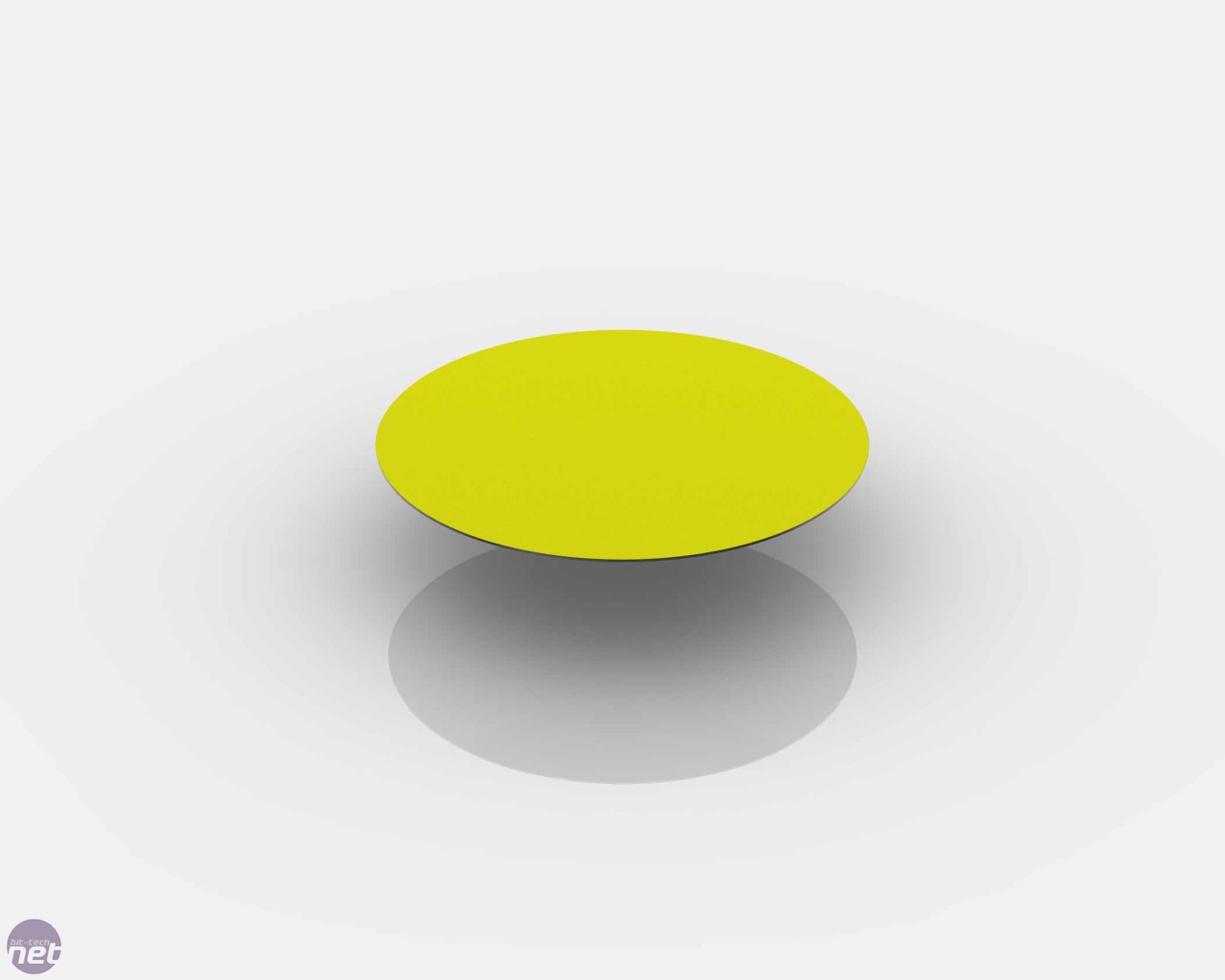
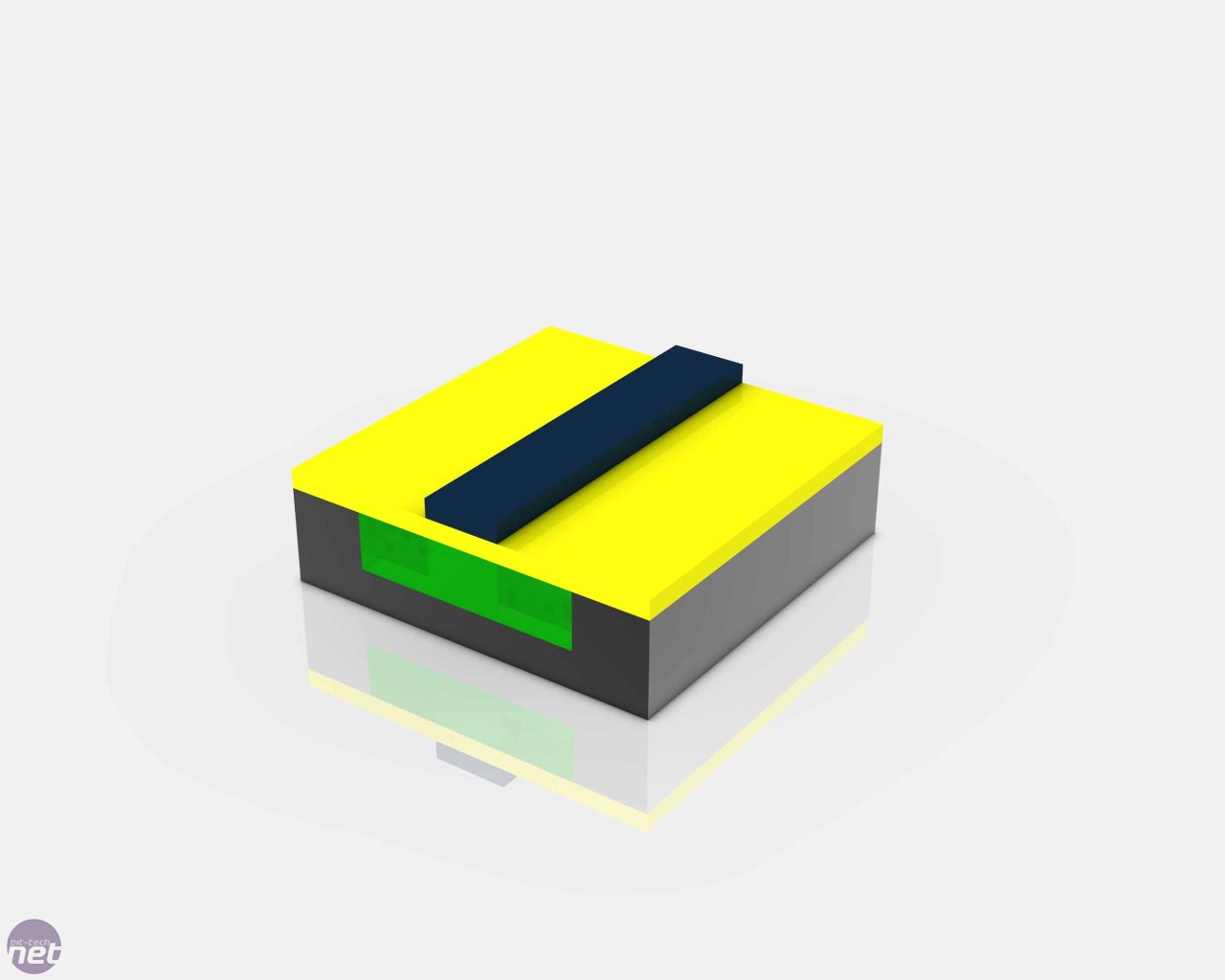
Left: The yellow sheets represent layers of High-K dielectric... obviously. Right: The dielectric is added in layers only one atom thick to give a perfect finish.
The dielectric is added in microscopic layers, literally only an atom thick at a time. Adding the dielectric in this manner allows greater accuracy and reduces potential electrical leakage, leading to more energy efficient processors in the long run.
The High-K material is also applied in a thicker layer than with traditional insulators, but still retains the same capacitive properties as these materials. This allows electrical leakage to be reduced (due to the thicker material) without affecting capacitive performance, a property which is key to making manufacturing at these tiny sizes possible.
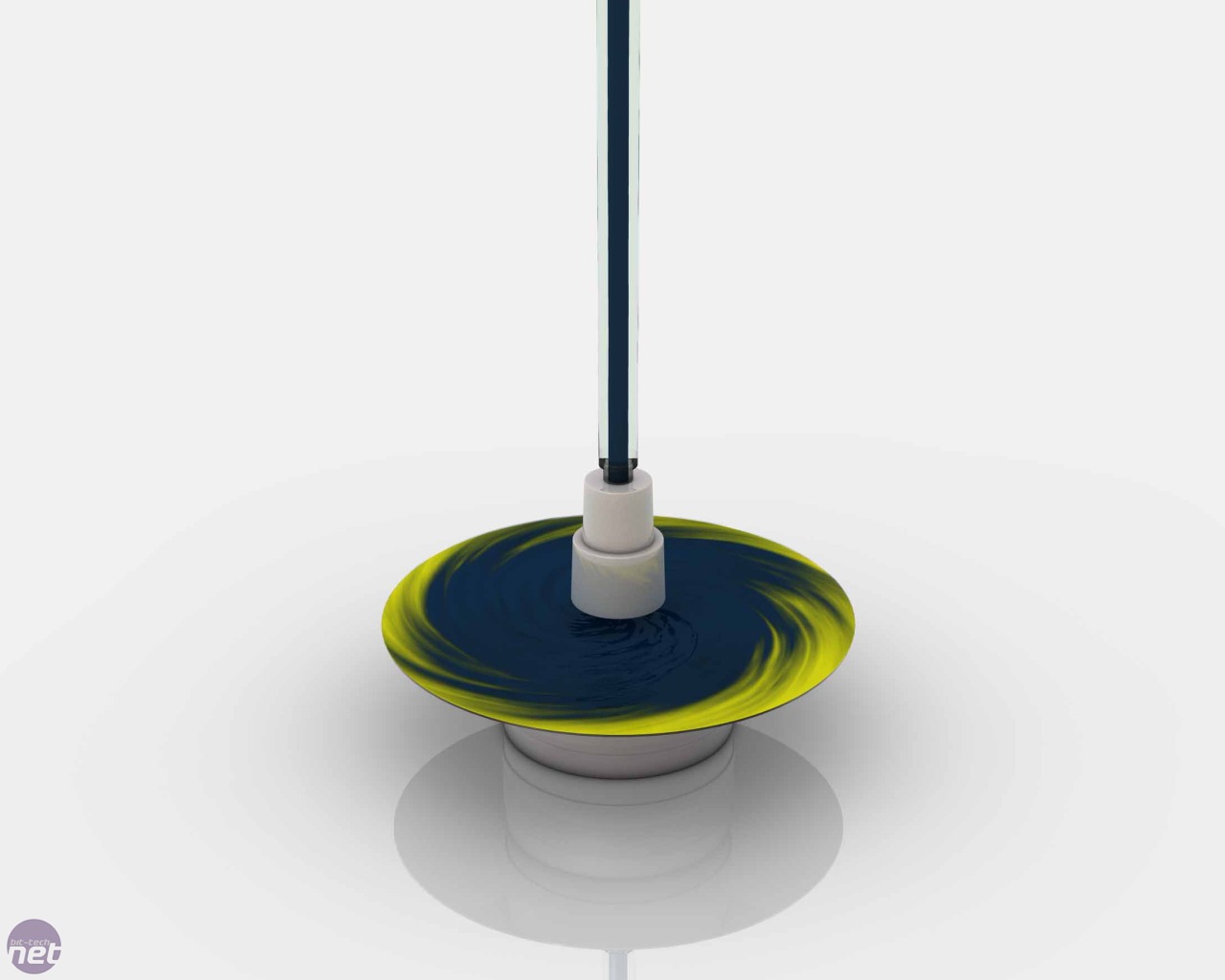
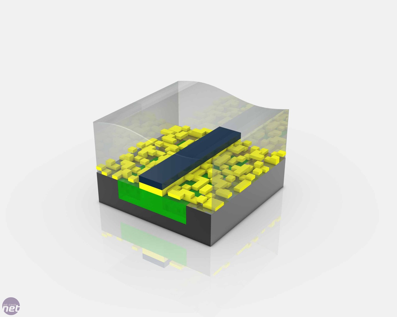
Left: The wafer is spun to distribute the photo resist evenly. Right: The masks used in the photo lithography are incredibly detailed.
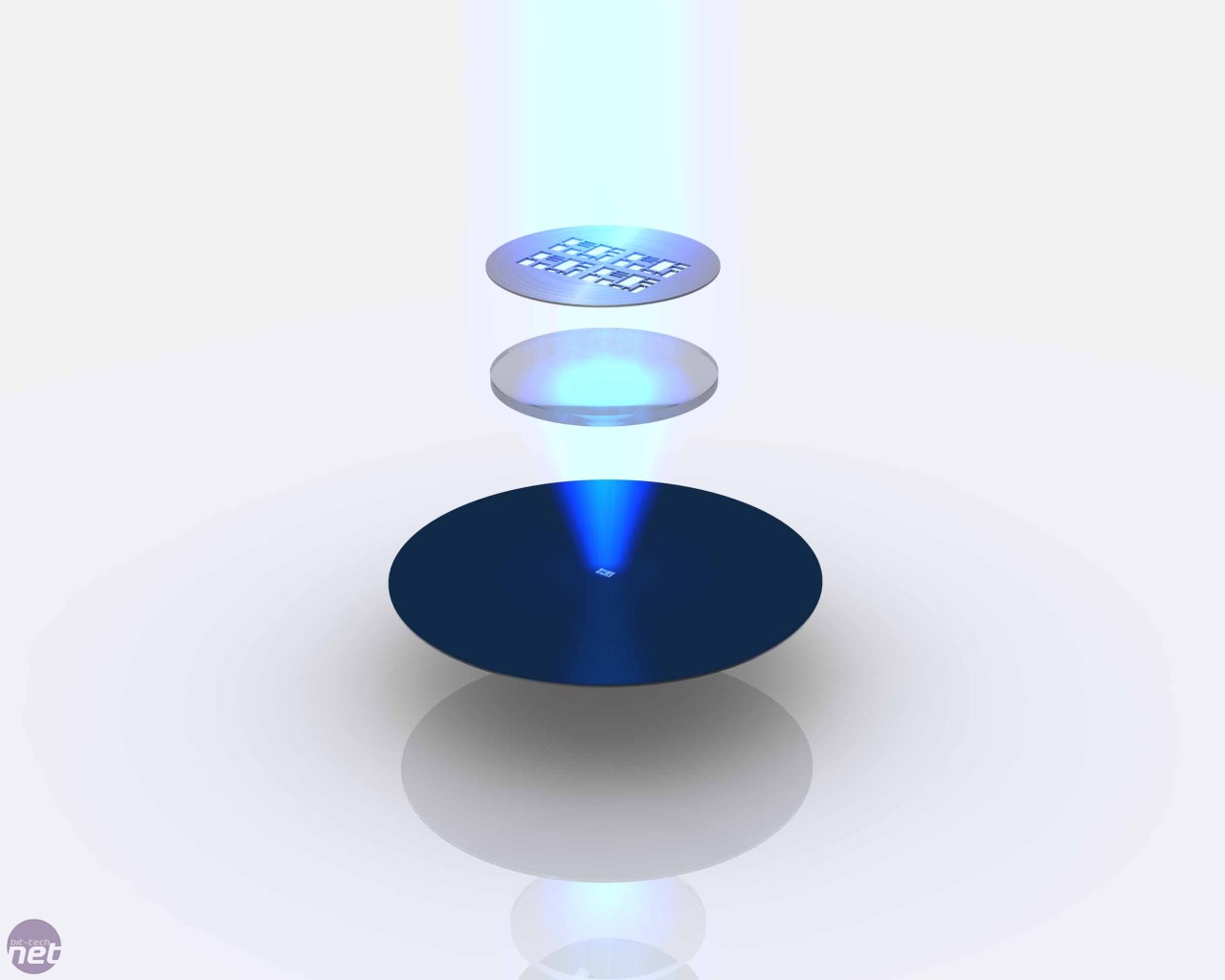
Another layer of photo resist is then added. The wafer is then exposed to a specific pattern of ultra violet light which turns sections of the photo resist soluble, in a process called photo lithography.
The pattern of light is achieved by using finely detailed ‘masks’, which act like stencils. These masks, detailed as they are, still need to be focused down to the microscopic levels that current CPUs work at. This is done by passing the masked light through a lens, which typically reduces the size of the mask's image by four times.
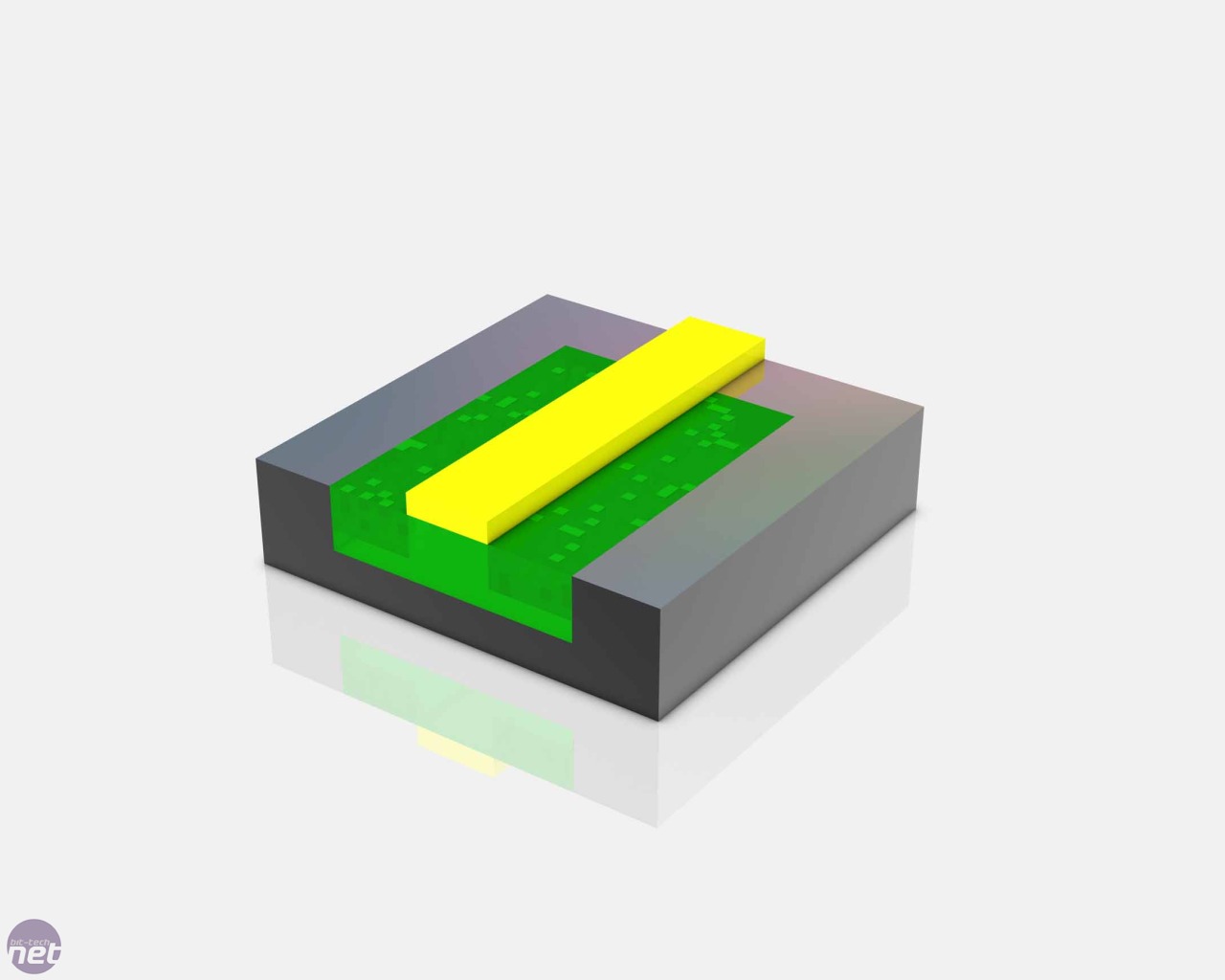
Left: We've zoomed down to look at a single transistor now. The dark line in the centre shows where the mask stopped the UV light reacting with the photo resist. Right: The UV-reacted photo resist is removed with gentle solvents.
The photo resist exposed to the light can now be removed with a solvent, leaving behind a specific pattern of unaffected photo resist created by the mask. This photo resist then protects the pattern of High-K dielectric it still covers, while the excess High-K material is gently etched away using chemicals.
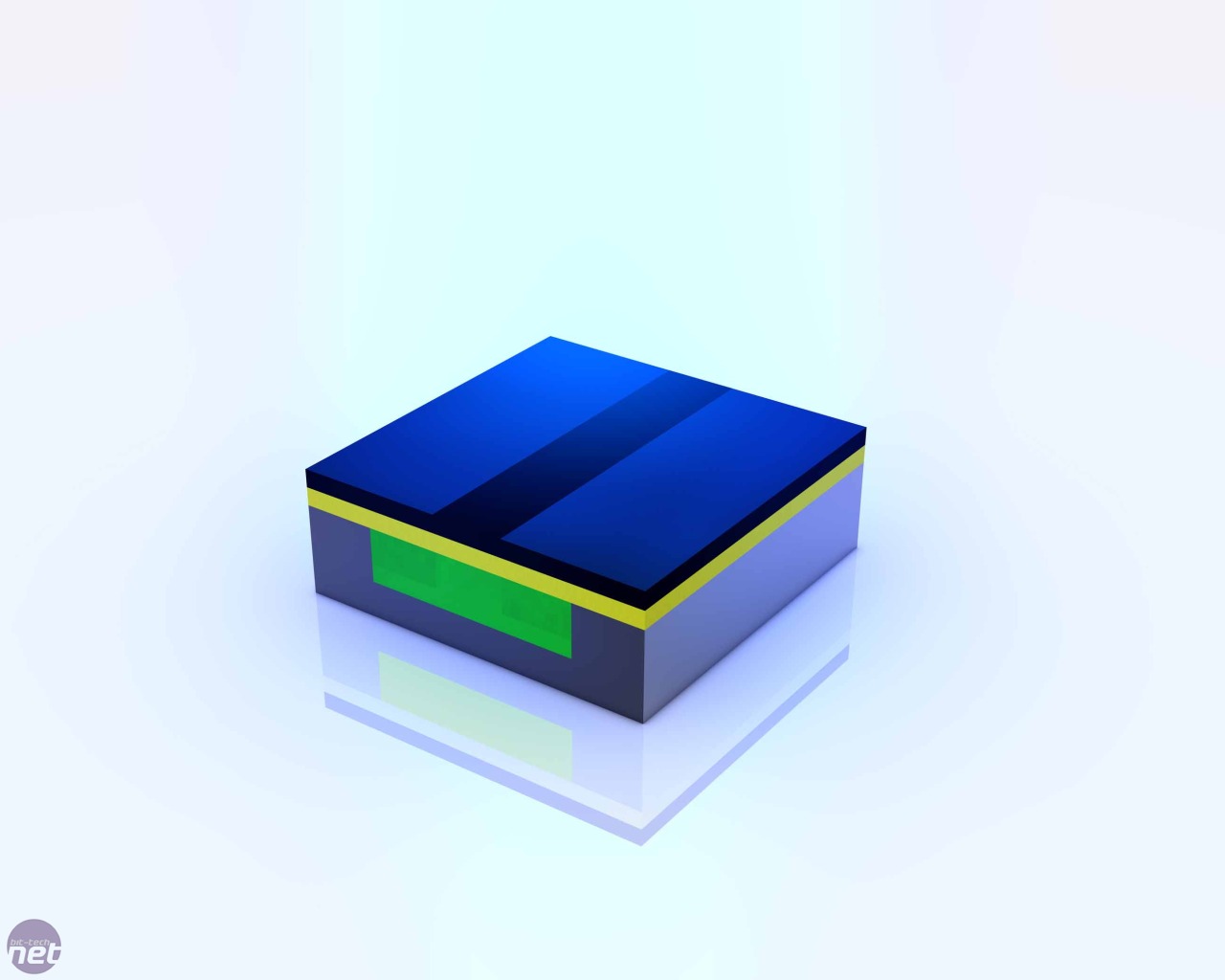
Left: The photo resist also resists the etching chemicals. Right: The yellow strip is the High-K dielectric, and the green is the doped conductive silicon
The photo resist is then removed leaving an incredibly intricate pattern of High-K dielectric on top of the conductive and non conductive silicon.
RELATED ARTICLES


MSI MPG Velox 100R Chassis Review
October 14 2021 | 15:04

Want to comment? Please log in.