What's New
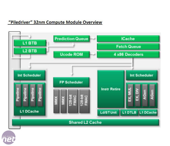
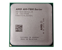
Without any change to the core architecture, we don't need to go into too much detail here, but a brief overview of what Richland comprises is still in order. As with Trinity, each 1.3 billion transistor chip will ship with either one or two Piledriver modules, and thus either two or four cores. In each of the modules, these two main cores are joined by a single floating point unit and a shared L2 data cache of up to 1MB per core.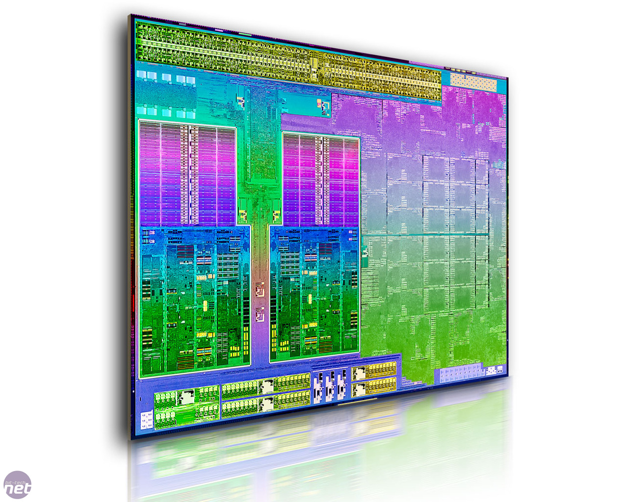
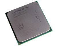
Click to enlarge - The Richland APUs have the same chip layout and Piledriver modules as Trinity
Communication with the system memory is achieved via two 64-bit memory controllers, so with 1,600MHz RAM, for example, the GPU will have a total memory bandwidth of 25.6GB/sec. The flagship model, the A10-6800K, is also now officially rated for 2,133MHz memory, while the rest of the range remains rated at 1,866MHz (although it may be possible to use higher frequencies via overclocking). While such speeds pale in comparison to the GDDR5 memory of discrete graphics cards, this is still good news for the onboard GPU, and we'll be testing the impact of faster memory on frame rates.
The GPU is based on the 4-way VLIW architecture originally found in the Radeon 6900 series of cards, so the Radeon HD 8000 nomenclature is for marketing purposes only. A fully enabled Cayman card features 24 SIMDs, but as with Trinity, Richland APUs have up to a maximum of 6, and thus contain up to 384 streaming processors (16 VLIW4 arrays per SIMD). The clock speed of our two chips is 844MHz, and this 44MHz increase over Trinity is

Click to enlarge
According to AMD, Turbo Core functionality has been much improved for Richland. One improvement is the addition of more voltage and frequency levels (operating points) so the integrated micro-controller can better choose performance for a certain workload, theoretically improving efficiency. The Turbo Core algorithms are also now able to detect when parts of the APU are bottlenecked and establish whether providing extra power will actually be beneficial. Finally, data from the new on-die temperature sensors around the CPU and GPU cores is also used to improve the accuracy of the power-based temperature calculations that the previous generation relied on.
Overclocking
While we run our benchmarks with the APUs are stock speeds, we also wanted to see how far we could push the two chips, and you'll find both stock and overclocked results in the performance graphs.We began by heading into the BIOS and disabling any power saving features (in our case, C6 and PowerNow) before increasing any VRM related settings to higher levels to hopefully allow for heftier overclocks. With this in mind, we also added a fan above the motherboard VRMs on our test bench, although most chassis exhaust fans should provide enough airflow to draw heat away from this area.
The absence of the K suffix on the A10-6700 indicates that its multiplier cannot be increased, but overclocking can still be achieved by increasing the base clock, which is 100MHz by
Click to enlarge
With the unlocked A10-6800K, we were able to hit a maximum stable frequency of 4.73GHz using 1.5V, a healthy 15 percent over the stock 4.1GHz. To reach this, we used a base clock of 110MHz and increased the multiplier to 43. As you're also able to increase the default GPU clock, we upped this to 894MHz, which becomes 983MHz thanks to the higher base clock. Our 1,600MHz memory at this setting runs at 1,760MHz, taking the GPU memory bandwidth to 28.2GB/sec.
RELATED ARTICLES


MSI MPG Velox 100R Chassis Review
October 14 2021 | 15:04

Want to comment? Please log in.