Zen 2: Under the Hood
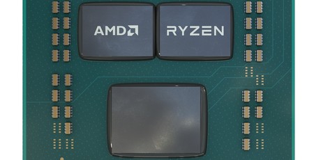
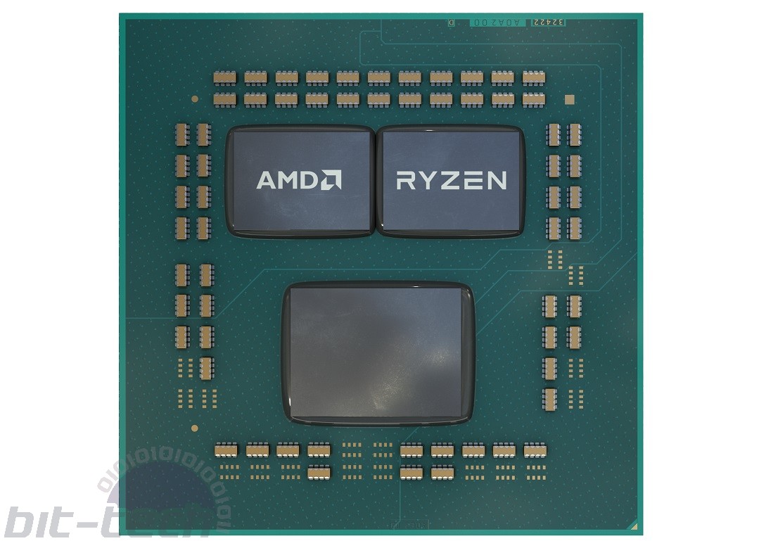
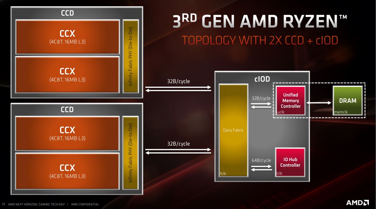
The chiplet design makes use of Core Die Chiplets (CCDs) that employ the 7nm manufacturing process and are each made up of a pair of four-core CPU Complexes (CCXs). As you can see below, there's space on the substrate for a pair of CCDs, giving rise to 12- and 16-core CPUs, namely the Ryzen 9 3900X and Ryzen 9 3950X. Additionally, an I/O die sits off to one side and, as scaling it down to 7nm proved troublesome, this remains at 12nm. The I/O die houses the likes of the improved dual-channel DDR4 memory controller, integrated southbridge, and PCIe 4.0 root-complex.
It's also easy to see how core counts can be increased quite easily using the same scale CCDs on the larger real estate provided by Threadripper CPUs, which we'll see at some point. Each 7nm CCX now occupies 31.3mm2, while a Zen+ CCX was nearly double the area at 60mm2 - very clearly a huge improvement that absolutely lends itself to higher core counts.
The chiplet design also lends itself to sharing the heat load over a wider area of the IHS compared to one large monolithic die, although that's only likely to benefit multi-threaded workloads seeing as the improved Windows Scheduler will fill a single CCX first before tipping over to others, containing loads into smaller spaces than they might otherwise be.
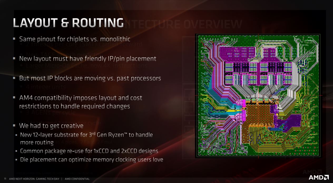
Despite the rather involved move to the 7nm chiplet design, the pinout is the same compared to previous generations, and thus AMD keeps compatibility with previous AM4 motherboards (take note, Intel). Admittedly, original first-gen Ryzen CPUs aren't supported in X570 boards, but we doubt you'd want to invest in a very pricey X570 model just to transplant a first-gen CPU anyway.
Key Architecture Improvements
The Zen 2 microarchitecture sports a bunch of improvements. From the top there's a new TAGE branch predictor, which holds almost twice the number of branches as previous generations. There's extra capacity in the micro-op cache, with the decode now handling 4K instructions as opposed to 2K previously, and perhaps most impressive of all are the much larger L3 cache amounts - double that of Zen+ and Zen.
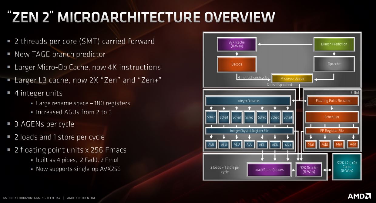
The hardware-managed SMT has been improved, plus we get a 50 percent boost to the Address Generation Unit (AGU) count, which leaps from two to three, and this should improve memory access efficiency. The floating point and load store bandwidths have increased from 128-bit to 256-bit for more efficient data movement, and if you use AVX-enabled applications then the move to processing AVX256 in a single operation or clock cycle is going to bring it more in line with Intel and - as with the expected gains in games thanks to better boosting, IPC, and thread handling - should offer similar increases in programs that benefit from AVX too.
Splash Some Cache
Not since Skylake-X have we seen such a rework of cache hierarchy compared to a previous generation of desktop CPUs, and while the latter went big on L2 cache, here AMD is beefing up the L3 cache and on a massive scale. Taking a step back for a moment, the L2 cache remains the same as Zen+ at 512KB per core or 2MB per CCX, while the L1 cache is also unchanged at 32KB but with double the load/store bandwidth.
Gamecache is a new term from AMD but essentially refers to the combined total of L2 and L3 cache. For example, the Ryzen 9 3900X's Gamecache is 70MB - an enormous amount - of which L2 cache makes up 2MB L2 cache per CCX. Two CCXs per CCD equates to 4MB L2 cache per CCD and 8MB L2 cache in total for the flagship Ryzen 9 3950X, but the Ryzen 9 3900X has 2MB less than the flagship (72MB total), as it essentially has an entire CCX disabled in dipping from 16 cores to 12.
This also explains why the six-core Ryzen 5 3600X has 1MB less L2 cache than the eight-core Ryzen 7 3700X; as two cores are disabled, you lose that 512KB L2 cache per core. The massive L3 cache is broken down to 4MB per core, 16MB per CCX - as we've mentioned that's double Zen and Zen+ - and 32MB per CCD assuming all cores are active. While large cache sizes often mean slightly higher latency, the benefit here is that you don't need to access memory as frequently.


MSI MPG Velox 100R Chassis Review
October 14 2021 | 15:04

Want to comment? Please log in.