
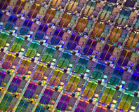
Toshiba is looking to steal a head start on its competitors with the news that the company has made a breakthrough which will see a 16nm process possible while others are still perfecting the 32nm size.
As reported over on TG Daily, the company is claiming that a breakthrough in the use of strontium germanide which allows metal-insulator-semiconductor field-effect transistors to be produced at a process size of 16nm or below – a previously challenging proposition.
The strontium germanide works as an interlayer in the silicon chips, and boost the current handling capabilities to levels that standard semiconductors can't match – allowing the chips to be shrunk beyond currently possible levels.
Although many companies are looking to strontium-based manufacturing processes as the limitations of silicon become ever more pressing, Toshiba believes it has solved one of the major implementation problems – the fabrication of a thin enough gate stack.
Although the technology is confined to the lab at present, Toshiba will be presenting a paper on its findings at the VLSI Symposia in Kyoto later this week – during which time we will, hopefully, get a hint of when the company expects to be bringing 16nm devices to market.
Looking forwards to seeing chips shrinking ever smaller, or does the future of technology lie elsewhere? Share your thoughts over in the forums.
RELATED ARTICLES


MSI MPG Velox 100R Chassis Review
October 14 2021 | 15:04

Want to comment? Please log in.