Wafer maker Soitech has announced a new fully depleted silicon wafer which, the company claims, makes it considerably easier and cheaper to build semiconductors using 3D transistors.
While Intel is on track to be the first to market with its Tri-Gate Transistor technology, fin-based Field Effect Transistors (FinFETs) have long been considered as the next big thing in semiconductor design. Unlike traditional planar transistors, FinFETs - a term coined by researchers from the University of California at Berkeley - are build on a silicon-on-insulator (SOI) substrate to create multigate transistors which extend into the third dimension.
A FinFET-based device promises a decrease in current leakage and a reduction in the short-channel effect as process sizes shrink to sub-20nm levels. The technology isn't without its issues, however: 3D transistors are significantly more complex to manufacture than planar transistors, with Intel thus far on track to be the first to push a related technology to market in a mass-produced semiconductor.
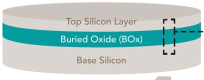
Soitec hopes to address the manufacturing issues that are preventing widespread use of FinFET designs with its new FD-3D wafer type. Constructed from a thin layer of silicon over a buried oxide layer, the silicon's thickness is customised according to the required fin height while the BOX layer provides isolation.
The result, Soitec claims, is a reduction in the number of steps required to manufacture 3D transistor-based semiconductors - translating directly into reduced costs, faster time to market and improved yields. According to the company's figures, companies using an FD-3D wafer over a traditional wafer type could see their products hit the market up to a year earlier.
'Our fully depleted product roadmap addresses the critical needs of the semiconductor industry and solves key challenges facing manufacturers today. Whichever path chip vendors choose to follow – planar or FinFET – Soitec provides solutions that address cost, performance, power-efficiency and time-to-market issues,' claimed Paul Boudre, chief operating officer of Soitec, at the announcement. 'FD-2D enables immediate and significant performance leaps, while FD-3D makes FinFET a reality for the entire industry at accelerated schedules and reduced risk.'
As well as its FD-3D and related planar FD-2D wafers, Soitec has announced plans to introduce strained silicon versions of its wafers. By modifying the crystalline structure of the silicon layer, Soitec claims, electron mobility can be improved - meaning a higher operating frequency for the finished device. The company is also investigating the use of germanium and nano-wire materials for expansion beyond the 14nm process size.
While Soitec's claims are impressive, the company has yet to confirm whether any tier one semiconductor companies have signed up to use the FD-3D wafers.
While Intel is on track to be the first to market with its Tri-Gate Transistor technology, fin-based Field Effect Transistors (FinFETs) have long been considered as the next big thing in semiconductor design. Unlike traditional planar transistors, FinFETs - a term coined by researchers from the University of California at Berkeley - are build on a silicon-on-insulator (SOI) substrate to create multigate transistors which extend into the third dimension.
A FinFET-based device promises a decrease in current leakage and a reduction in the short-channel effect as process sizes shrink to sub-20nm levels. The technology isn't without its issues, however: 3D transistors are significantly more complex to manufacture than planar transistors, with Intel thus far on track to be the first to push a related technology to market in a mass-produced semiconductor.
Soitec hopes to address the manufacturing issues that are preventing widespread use of FinFET designs with its new FD-3D wafer type. Constructed from a thin layer of silicon over a buried oxide layer, the silicon's thickness is customised according to the required fin height while the BOX layer provides isolation.
The result, Soitec claims, is a reduction in the number of steps required to manufacture 3D transistor-based semiconductors - translating directly into reduced costs, faster time to market and improved yields. According to the company's figures, companies using an FD-3D wafer over a traditional wafer type could see their products hit the market up to a year earlier.
'Our fully depleted product roadmap addresses the critical needs of the semiconductor industry and solves key challenges facing manufacturers today. Whichever path chip vendors choose to follow – planar or FinFET – Soitec provides solutions that address cost, performance, power-efficiency and time-to-market issues,' claimed Paul Boudre, chief operating officer of Soitec, at the announcement. 'FD-2D enables immediate and significant performance leaps, while FD-3D makes FinFET a reality for the entire industry at accelerated schedules and reduced risk.'
As well as its FD-3D and related planar FD-2D wafers, Soitec has announced plans to introduce strained silicon versions of its wafers. By modifying the crystalline structure of the silicon layer, Soitec claims, electron mobility can be improved - meaning a higher operating frequency for the finished device. The company is also investigating the use of germanium and nano-wire materials for expansion beyond the 14nm process size.
While Soitec's claims are impressive, the company has yet to confirm whether any tier one semiconductor companies have signed up to use the FD-3D wafers.


MSI MPG Velox 100R Chassis Review
October 14 2021 | 15:04

Want to comment? Please log in.