Samsung, TSMC unveil sub-7nm EUV nodes
April 17, 2019 | 10:25
Companies: #samsung #taiwan-semiconductor
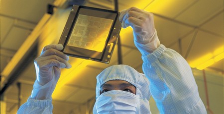
Samsung and Taiwan Semiconductor (TSMC) have both announced successful development of their next-generation semiconductor process nodes, 5nm and 6nm respectively, both using extreme ultraviolet (EUV) lithography.
The march of Moore's Law, the observation by Intel co-founder Gordon Moore that the number of transistors on a leading-edge part trends towards a doubling roughly every eighteen months, has necessitated a constant shrinking of the size of those parts - lest we end up with processors the size of football fields. As process nodes drop into the single-digit nanometres, however, each shrinkage becomes increasingly difficult - Intel has been struggling for years to ramp its 10nm node, while AMD manufacturing spin-out GlobalFoundries put its own 7nm programme on indefinite hold late last year.
Samsung and Taiwan Semiconductor (TSMC), by contrast, claim to have everything down-pat for their respective next-generation process node shrink. In both cases the companies are using extreme ultraviolet (EUV) lithography, which uses a shorter wavelength of light than traditional photolithographic processes in order to handle ever-shrinking component sizes.
Samsung's offering, building on the 7nm EUV node it unveiled in October 2018, is a 5nm node which it claims offers a 20 percent improvement in power consumption or 10 percent improvement in performance - or a mixture of the two - compared to the same parts built on its 7nm process node.
'In successful completion of our 5nm development, we've proven our capabilities in EUV-based nodes,' crows Charlie Bae, executive vice president of Samsung Electronics' foundry business unit. 'In response to customers' surging demand for advanced process technologies to differentiate their next-generation products, we continue our commitment to accelerating the volume production of EUV-based technologies. Considering the various benefits including PPA [power performance area] and IP [intellectual property], Samsung's EUV-based advanced nodes are expected to be in high demand for new and innovative applications such as 5G, artificial intelligence (AI), high performance computing (HPC), and automotive. Leveraging our robust technology competitiveness including our leadership in EUV lithography, Samsung will continue to deliver the most advanced technologies and solutions to customers.'
The company's 5nm process is joined by a 6nm customised node, again based on EUV lithography, which Samsung claims has already received its first tape-out. While it boasts of existing EUV production in its Hwaseong fab and a new EUV line to be opened in the second half of the year, however, the company has not offered a timescale for volume production on either the 5nm or custom 6nm nodes.
Rival TSMC, meanwhile, has announced an EUV process of its own, based on a 6nm node. Boosting logic density by around 18 percent, the new node is designed as a successor to the company's 7nm N7+ process - and, as with Samsung's next-generation process node, the company promises an easy transition from 7nm for existing customers. 'TSMC N6 technology will further extend our leadership in delivering product benefits with higher performance and cost advantage beyond the current N7,' claims Dr. Kevin Zhang, TSMC vice president for business development. 'Building upon the broad success of our 7nm technology, we're confident that our customers will be able to quickly extract even higher product value from the new offering by leveraging a well-established design ecosystem today.'
Unlike Samsung, however, TSMC is willing to put a date on the first chips to appear based on its new node: Risk production, the company explains, is scheduled for the first quarter of 2020, though it has not yet issued a timescale for ramp-up to volume production.


MSI MPG Velox 100R Chassis Review
October 14 2021 | 15:04

Want to comment? Please log in.