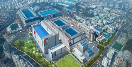
Samsung has announced that it has started wafer production on its 7nm Low Power Plus (7LPP) process node, based on extreme ultraviolet (EUV) lithography, and pledges a 'definite path to 3nm'.
The constant march of Moore's Law, the observation turned hard target by Intel co-founder Gordon Moore that the number of transistors on a leading-edge part trends towards a doubling every 18 months, has necessitated a constant shrinking of the node on which they are produced - not only as a means of improving performance and lowering power draw, but also to avoid current-generation processors from being the size of a football pitch. As manufacturers hit 10nm and below, though, the process becomes increasingly difficult - as Intel knows only too well, having delayed its own full 10nm node launch by four years and counting.
One approach to solving some of the issues relating to building semiconductors at 10nm and below is extreme ultraviolet (EUV) lithography, which uses light wavelengths around the 13.5nm mark at extremely high energy levels to allow for finer patterns to be transferred than traditional photolithography and in a single mask rather than requiring multiple-mask patterning. It brings its own difficulties, though, but difficulties that Samsung claims to have resolved with the launch of its EUV-based 7nm Low Power Plus (7LPP) process node.
'With the introduction of its EUV process node, Samsung has led a quiet revolution in the semiconductor industry,' crows Samsung's Charlie Bae of the company's breakthrough. 'This fundamental shift in how wafers are manufactured gives our customers the opportunity to significantly improve their products' time to market with superior throughput, reduced layers, and better yields. We're confident that 7LPP will be an optimal choice not only for mobile and HPC [high-performance computing], but also for a wide range of cutting-edge applications.'
According to Samsung's internal testing, parts built on 7LPP will benefit from a 40 percent area-efficiency increase, 20 percent performance increase, or a 50 percent reduction in power requirements when compared with the company's 10nm FinFET process. At the same time, the company announced 7LPP ready partnerships in the Samsung Advanced Foundry Ecosystem (SAFE) programme, including process design kits (PDKs), intellectual properties, reference flows, packaging solutions, and design services ready for 7LPP use.
Thus far, neither Samsung nor its customers have indicated when the first commercial products based on the 7LPP process will be arriving on shop shelves.


MSI MPG Velox 100R Chassis Review
October 14 2021 | 15:04

Want to comment? Please log in.