Researchers announce microwave-based chip imaging breakthrough
July 4, 2017 | 10:55
Companies: #epf-lausanne #eth-zurich #johannes-kepler-university #keysight-technologies #paul-scherrer-institut #research #university-college-london
A team of researchers working with the University College London (UCL) has announced a claimed breakthrough in investigating the internal workings of modern silicon semiconductors, allowing images to be taken of their internals without destroying the component.
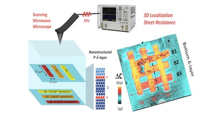
The team, comprised of researchers from UCL, Johannes Kepler University, Keysight Technologies, the Paul Scherrer Institut, ETH Zürich, and EPF Lausanne, worked to create imagery of three-dimensional components constructed from phosphorus atoms buried deep inside a semiconductor chip - components entirely invisible to all existing non-destructive imaging technologies such as ultrasound and X-ray. The parts, atomically thin and mere tens of atoms wide, were laid down using a metal needle 'writing' hydrogen atoms onto a silicon chip which was then chemically treated to deposit phosphorus atoms via phosphine gas before being buried with additional silicon - making them invisible to all existing non-destructive imaging techniques.
When it came time to view the structures, the team used a metal needle pushed against the surface of the chip to beam focused microwaves into the silicon and read the resulting bounce-back - resulting in accurate images of the structures without destroying the component. 'The work is potentially of global significance because silicon chips are becoming so sophisticated and intricate that taking snapshots of their smallest working parts is incredibly difficult and time consuming, and currently involves destroying the chip,' explained UCL's Dr. Neil Curson, of the University's London Centre for Nanotechnology, regarding his team's contribution to the project. 'If we could easily see all components of a chip, in a non-destructive manner, it would be a game-changer. What we have done is a big step towards just that. Such technologies are also becoming important for governments who are interested in knowing what is inside the foreign electronics they are using!'
The team has also suggested that the imaging system could aid with the construction of quantum processors based around phosphorus-in-silicon technology, though none of the researchers involved have pointed towards a commercialisation date. The full paper can be read free of charge courtesy of the Science Advances journal Volume 3 Number 6.


MSI MPG Velox 100R Chassis Review
October 14 2021 | 15:04

Want to comment? Please log in.