IDF 2010 Following on from our original news story, Intel has now started to confirm more technical details about the architecture of its forthcoming Sandy Bridge CPUs.
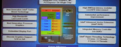
One of the most interesting of these is the new integrated GPU. For example, Intel has revealed that although it has a similar number of stream processors (or as Intel likes to call them 'execution units') to it's current-generation integrated GPU of existing Core i3 and i5 CPUs, the stream processors will have twice the throughput.
However, Intel reckons the biggest performance boost comes from switching the GPU from using system memory as its main repository of data to the Level 3 cache inside the CPU. Although this means that Intel has had to create all sorts of rules so that the CPU cores and GPU do not fight for access to the cache, as the cache delivers approximately four times the bandwidth of system memory, the system as a whole is much faster.
Intel described the process of creating these rules as 'thinking of the GPU as a fifth CPU core' not a separate unit. Using the cache has another benefit too: as the memory controller and system memory isn't being used it also saves a lot of power.
It's worth noting that most modern games will need considerably more texture memory than the Level 3 cache of a CPU can provide, so the Sandy Bridge GPU will still need to use system memory as well in these situations.
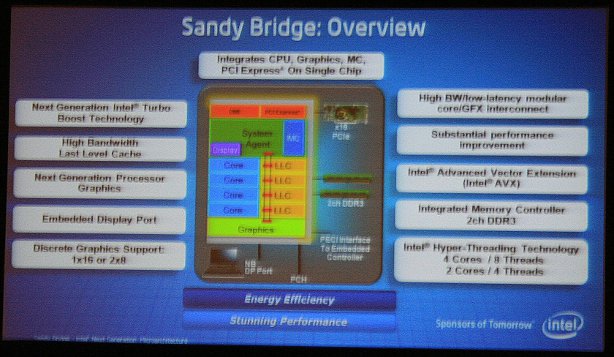
It was necessary for Intel to design this ring interconnect because the CPU cores and GPU in Sandy Bridge are built together on one die, which will use the 32nm manufacturing process. In contrast, existing Core i3 and Core i5 CPUs are built on a 32nm die and then patched together with a 45nm GPU. The ring interconnect is not only much faster than the existing QPI and DMI buses, but it should also enable Intel to ship variations on the basic Sandy Bridge design very quickly, such as models with different numbers of CPU cores.
Intel has also been talking about the enhanced form of Turbo Boost in Sandy Bridge. Specifically, unlike existing Bloomfield and Lynnfield CPUs, which can only overclock 1-2 CPU cores, Sandy Bridge CPUs can overclock all four cores simultaneously. What's more, the on-board GPU also supports Turbo Boost, although it can't overclock itself at the same time as the CPU cores. Confusingly, this means that Sandy Bridge CPUs can easily exceed their rated TDP, although Intel couldn't confirm what the point of having a TDP is if it can be exceeded.
Finally, Intel has been talking briefly about the new AVX (Advanced Vector Instructions). This is a new set of 256-bit instructions designed to enhance floating-point performance when handling media files, such as video and photo editing.
Beyond confirming that there will be dual- and quad-core models, Intel isn't talking clock speeds or model numbers for Sandy Bridge yet, although it did mention special low-power models with a TDP as low as 35W - much lower than most modern CPUs. Whether or not this low TDP will be exceeded via the new Turbo Boost remains to be seen.
Does Sandy Bridge sound like it's shaping up nicely? Share your thoughts in the forum.
One of the most interesting of these is the new integrated GPU. For example, Intel has revealed that although it has a similar number of stream processors (or as Intel likes to call them 'execution units') to it's current-generation integrated GPU of existing Core i3 and i5 CPUs, the stream processors will have twice the throughput.
However, Intel reckons the biggest performance boost comes from switching the GPU from using system memory as its main repository of data to the Level 3 cache inside the CPU. Although this means that Intel has had to create all sorts of rules so that the CPU cores and GPU do not fight for access to the cache, as the cache delivers approximately four times the bandwidth of system memory, the system as a whole is much faster.
Intel described the process of creating these rules as 'thinking of the GPU as a fifth CPU core' not a separate unit. Using the cache has another benefit too: as the memory controller and system memory isn't being used it also saves a lot of power.
It's worth noting that most modern games will need considerably more texture memory than the Level 3 cache of a CPU can provide, so the Sandy Bridge GPU will still need to use system memory as well in these situations.
New Ring Interconnect
Probably the most interesting aspect of Sandy Bridge's design that Intel revealed today is its ring interconnect. Comprising 1,000 traces, this new bus, which delivers up to 96GB/sec per link, is based on the ring bus inside the Xeon 7500-series of CPUs and is used to connect the CPU cores, GPU, memory controller and Level 3 cache.It was necessary for Intel to design this ring interconnect because the CPU cores and GPU in Sandy Bridge are built together on one die, which will use the 32nm manufacturing process. In contrast, existing Core i3 and Core i5 CPUs are built on a 32nm die and then patched together with a 45nm GPU. The ring interconnect is not only much faster than the existing QPI and DMI buses, but it should also enable Intel to ship variations on the basic Sandy Bridge design very quickly, such as models with different numbers of CPU cores.
CPU Upgrades
Intel also revealed some details about the core improvements inside the CPU portion of Sandy Bridge. The most notable of these is the ability of a Sandy Bridge CPU to load/store two addresses simultaneously, as opposed to the single address store of previous generation Intel processors.Intel has also been talking about the enhanced form of Turbo Boost in Sandy Bridge. Specifically, unlike existing Bloomfield and Lynnfield CPUs, which can only overclock 1-2 CPU cores, Sandy Bridge CPUs can overclock all four cores simultaneously. What's more, the on-board GPU also supports Turbo Boost, although it can't overclock itself at the same time as the CPU cores. Confusingly, this means that Sandy Bridge CPUs can easily exceed their rated TDP, although Intel couldn't confirm what the point of having a TDP is if it can be exceeded.
Finally, Intel has been talking briefly about the new AVX (Advanced Vector Instructions). This is a new set of 256-bit instructions designed to enhance floating-point performance when handling media files, such as video and photo editing.
Beyond confirming that there will be dual- and quad-core models, Intel isn't talking clock speeds or model numbers for Sandy Bridge yet, although it did mention special low-power models with a TDP as low as 35W - much lower than most modern CPUs. Whether or not this low TDP will be exceeded via the new Turbo Boost remains to be seen.
Does Sandy Bridge sound like it's shaping up nicely? Share your thoughts in the forum.
RELATED ARTICLES


MSI MPG Velox 100R Chassis Review
October 14 2021 | 15:04

Want to comment? Please log in.