
AMD has finally revealed firm details of its upcoming processor roadmap, including promises of significant performance boosts from its Zen microarchitecture due to replace Bulldozer and its related designs.
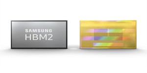
Speaking at the AMD financial analysts' event, Mark Papermaster admitted that the Bulldozer design - an architecture similar in concept to Intel's failed NetBurst and using a shared-FPU modular design many found troubling in highly-parallel workloads - had some issues regarding performance. Zen, as the company has been hinting for some time, is the answer. An entirely new core design, ditching the Bulldozer microarchtecture altogether, Zen is claimed to boost instructions per cycle (IPC) by 40 per cent compared to the previous-generation Excavator design, and includes true simultaneous multithreading (SMT) support and high-bandwidth memory (HBM) for low-latency caching. The design is also claimed to be considerably more energy efficient than its predecessor, thanks to a drop to a 14nm process node and the adoption of FinFET three-dimensional transistors - equivalent to the Tri-Gate Transistor technology Intel has been putting in its chips for a while now.
Papermaster also spoke briefly about K12, AMD's 64-bit ARM-architecture cores aimed at the microserver market. Although no new specifications were provided, AMD did admit to a slip in schedule that will see the first K12 chips released some time in 2017 - although Papermaster was keen to reaffirm his company's commitment to launching the first x86 Zen products in 2016.
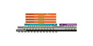
The Zen CPUs won't be the only devices to benefit from High-Bandwidth Memory (HBM): as previously suggested, AMD's next-generation graphics products will include HBM located next to the GPU on a shared interposer, a shift which will reduce latency and improve performance. All told, Papermaster claimed, the next-generation Graphics Core Next (GCN) parts will boast a two-fold performance-per-watt improvement over existing parts, although they are expected to remain on the 28nm process node for the time being.
'We see strong long-term growth opportunities across a diverse set of markets for the kind of high-performance compute and visualisation capabilities only AMD can provide,' claimed AMD president and CEO Lisa Su at the event, attempting to allay investors' concerns regarding the financial stability of the company. 'We are focusing our investments on our strongest opportunities to enable our customers to create great products that push the boundaries of what is possible and allow AMD to achieve profitable growth in the years to come.'
Additional mainstream roadmap shifts announced by AMD included the promise of new FX-series parts based on the Zen core with DDR4 compatibility and using the AM4 socket architecture, which will be shared with the desktop APUs launched in the same year. These desktop parts will be joined by seventh-generation APUs offering full HSA support and claims of discrete-class graphics performance in the ultra-thin FP4 format for mobile devices.
The company also announced new APU and Radeon GPU products aimed at OEMs, the former based on the Carrizo-L design and ranging from 10W to 25W TDPs and up to four cores at 2.5GHz and the latter comprised of the 300 Series and M300 Series for desktops and laptops respectively. From the 10th of May, the company will also be dropping the pricing of its A-Series APUs, with the top-end A10-7850K hitting a $127 manufacturer's recommended retail price (around £83 excluding tax.).
Full information on the announcements is available at AMD's official 2015 Financial Analyst Day microsite.
Speaking at the AMD financial analysts' event, Mark Papermaster admitted that the Bulldozer design - an architecture similar in concept to Intel's failed NetBurst and using a shared-FPU modular design many found troubling in highly-parallel workloads - had some issues regarding performance. Zen, as the company has been hinting for some time, is the answer. An entirely new core design, ditching the Bulldozer microarchtecture altogether, Zen is claimed to boost instructions per cycle (IPC) by 40 per cent compared to the previous-generation Excavator design, and includes true simultaneous multithreading (SMT) support and high-bandwidth memory (HBM) for low-latency caching. The design is also claimed to be considerably more energy efficient than its predecessor, thanks to a drop to a 14nm process node and the adoption of FinFET three-dimensional transistors - equivalent to the Tri-Gate Transistor technology Intel has been putting in its chips for a while now.
Papermaster also spoke briefly about K12, AMD's 64-bit ARM-architecture cores aimed at the microserver market. Although no new specifications were provided, AMD did admit to a slip in schedule that will see the first K12 chips released some time in 2017 - although Papermaster was keen to reaffirm his company's commitment to launching the first x86 Zen products in 2016.
The Zen CPUs won't be the only devices to benefit from High-Bandwidth Memory (HBM): as previously suggested, AMD's next-generation graphics products will include HBM located next to the GPU on a shared interposer, a shift which will reduce latency and improve performance. All told, Papermaster claimed, the next-generation Graphics Core Next (GCN) parts will boast a two-fold performance-per-watt improvement over existing parts, although they are expected to remain on the 28nm process node for the time being.
'We see strong long-term growth opportunities across a diverse set of markets for the kind of high-performance compute and visualisation capabilities only AMD can provide,' claimed AMD president and CEO Lisa Su at the event, attempting to allay investors' concerns regarding the financial stability of the company. 'We are focusing our investments on our strongest opportunities to enable our customers to create great products that push the boundaries of what is possible and allow AMD to achieve profitable growth in the years to come.'
Additional mainstream roadmap shifts announced by AMD included the promise of new FX-series parts based on the Zen core with DDR4 compatibility and using the AM4 socket architecture, which will be shared with the desktop APUs launched in the same year. These desktop parts will be joined by seventh-generation APUs offering full HSA support and claims of discrete-class graphics performance in the ultra-thin FP4 format for mobile devices.
The company also announced new APU and Radeon GPU products aimed at OEMs, the former based on the Carrizo-L design and ranging from 10W to 25W TDPs and up to four cores at 2.5GHz and the latter comprised of the 300 Series and M300 Series for desktops and laptops respectively. From the 10th of May, the company will also be dropping the pricing of its A-Series APUs, with the top-end A10-7850K hitting a $127 manufacturer's recommended retail price (around £83 excluding tax.).
Full information on the announcements is available at AMD's official 2015 Financial Analyst Day microsite.


MSI MPG Velox 100R Chassis Review
October 14 2021 | 15:04

Want to comment? Please log in.