Intel has released additional details of its upcoming Lakefield processor family, the first to be based on the company's Foveros three-dimensional packaging technology - and has promised it will enter production this year.
Intel's Foveros packaging technology was unveiled late last year as a logical extension to the 'chiplet' multi-die concept: Where traditional processors are a single die on a chip, and chiplet systems multiple dies spread out on a planar two-dimension surface connected using embedded bridges, Foveros extends the concept in three dimensions. Individual chiplets, offering compute, vision, or other application-specific capabilities, are connected on top of a base compute die and interposer, which is then connected to the package underneath. The technology uses a combination of face-to-face micro-bump solder points and through-silicon vias (TSVs), and the company claims offers improved bandwidth and reduced power draw compared to rival chiplet designs.
During the announcement, Intel teased its first Foveros product: A 'hybrid x86 architecture' designed dubbed Lakefield, targeting ultra-mobile devices, which combines a package, 22nm P1222 interposer and system-on-chip die, and P1274 10nm-based compute die with package-on-package (POP) memory for a low-footprint 12mmx12mmx1mm device.
Now, the company has released a brief video, reproduced above, hyping up the Lakefield release a little more, 'This hybrid CPU architecture enables combining different pieces of IP that might have previously been discrete into a single product with a smaller motherboard footprint,' the company's description explains, 'which allows OEMs more flexibility for thin and light form factor design.'
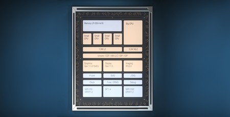
In the video, Lakefield's compute chiplet is confirmed as combining four small CPU cores with a single big Sunny Cove architecture CPU core - echoes of Arm's successful big.LITTLE architecture - alongside 1.5MB of L2 cache and 4MB of last-level cache (LLC), LP-DDR4 memory, Intel Graphics Gen 11-Low Power (Gen 11-LP), a Gen 11.5 display processor, imaging processor, and MIPI Display Serial Interface, Camera Serial Interface, and DisplayPort 1.4 components, along with miscellaneous glue logic and debugging interfaces.
'The result,' the promotional video crows, 'is a product that is optimised for power efficiency, immersive graphics, I/O, and memory, all in this tiny SoC which is approximately 12mm square.' That chip, the company further teases, can be installed on a motherboard measuring just 125mm by 30mm - approximately the length of a standard ball-point pen. The video also showcases some concept designs in which Lakefield could appear, including twin-screen convertible laptops and portrait-format 'book' devices.
While Intel has confirmed it plans to produce Lakefield parts by the end of the year, the company has not discussed pricing nor commercial availability.


MSI MPG Velox 100R Chassis Review
October 14 2021 | 15:04

Want to comment? Please log in.