Chip imaging breakthrough aids defect detection
October 8, 2019 | 11:07
Companies: #paul-scherer-institut #university-of-southern-california
Researchers at the Paul Scherer Institut in Switzerland the University of Southern California's Viterbi School of Engineering have announced a breakthrough in the detection of physical flaws in modern processors - while also promising easier reverse engineering, something many companies will not be welcoming.
The march of Moore's Law, which started life as an observation by Intel co-founder Gordon Moore that the number of transistors on a leading-edge part trends towards a doubling every 18 months and has since become a must-hit target for the semiconductor industry, has resulted in ever-growing number of ever-shrinking parts on a modern processor. Defects in the parts are a problem, and detecting said defects becomes harder the more parts they are and the smaller they get.
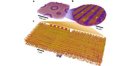
Researchers at the Paul Scherer Institut in Switzerland the University of Southern California's Viterbi School of Engineering have demonstrated a new technique, ptychographic x-ray laminography, which they claim can detect flaws better than any current technique - and could also make reverse-engineering a part non-destructively possible.
The technique works by rotating a chip at a 61-degree angle and illuminating small regions using x-rays from a synchrotron; the resulting diffraction patterns are then measured using a photon-counting detector array. The data from the array are then combined to create high-resolution slices of how the chip looks internally, which are then combined themselves into a three-dimensional rendering.
The chief reason for the development of the technique is fault detection: A production chip can be easily compared to the original design to see if it's within tolerance, and any defects highlighted. It also offers new opportunities for forensic investigations, with the researchers pointing out that the images show that images show signature features revealing where a chip was made and on what manufacturing process.
A bigger issue, though, is that the same technique can be used to reverse engineer a commercial part without the usual issues associated with the process of de-capping and dissolving the package to reveal the underlying circuitry. 'The majority of a chip's intelligence is how it is wired. It is like the connectome of a brain,' explains co-author Anthony Levi. 'By viewing a chip in detail, you can non-destructively figure out what it does. With this technology, hiding intellectual property in a chip is over.'
The team's work has been published in the journal Nature Electronics.


MSI MPG Velox 100R Chassis Review
October 14 2021 | 15:04

Want to comment? Please log in.