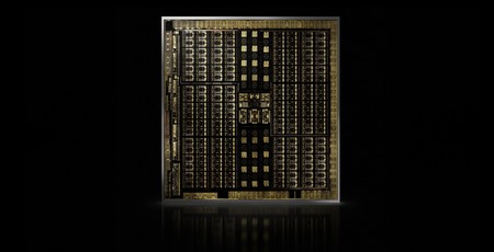
With Nvidia’s Volta architecture having been skipped on the consumer GeForce front, only finding its way into the prosumer-grade Titan V, workstation-grade Quadro GV100, and the Xavier generation of Tegra SoCs that focus on self-driving cars, the next green team architecture gamers can expect to use after Pascal is Turing, which will be powering the recently announced GeForce RTX 2000 series of graphics cards.
Today, we’re able at last to bring you full details of the Turing architecture and the specifications of the RTX 2080 Ti, RTX 2080, and RTX 2070, although performance data is still bound by NDA. As a reminder, the RTX 2080 Ti and RTX 2080 launch this month, while the RTX 2070 isn’t launching until October.
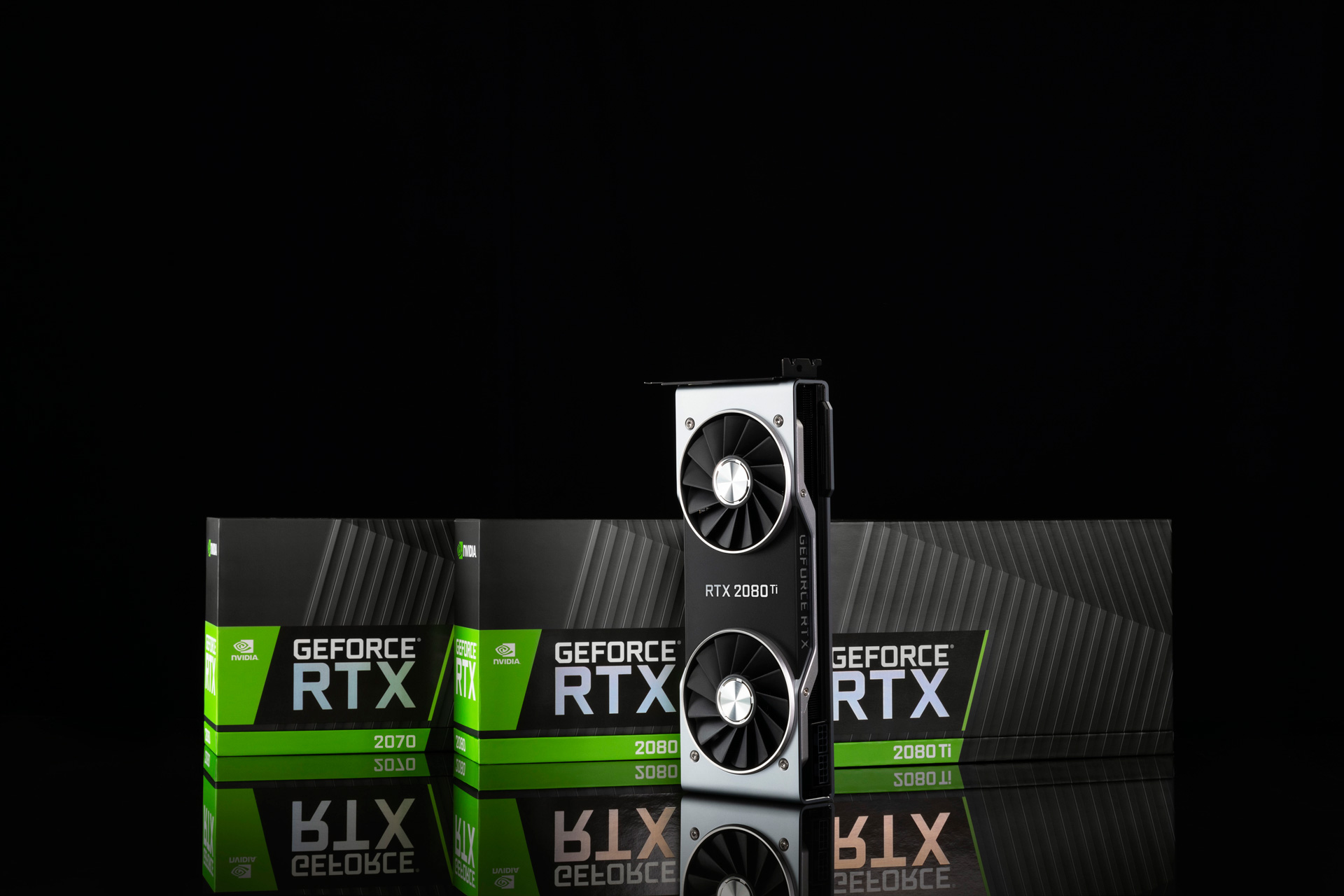
As you’ll see, there’s plenty to cover; this is a summary of information provided by Nvidia in an 83-page whitepaper and a full day of press-only presentations, so you may want to grab a cup of [insert caffeinated beverage of choice] before getting into the nitty gritty. However, we reckon a good place to start is with the full specifications of the three upcoming cards. After all, who doesn’t love a bloody good spec table?
(Note that Nvidia Founders Edition card specifications will differ slightly to these reference specs on account of their higher boost clocks, which are used to inform the TFLOPS, TIPS, RTX-OPS, and TDP calculations.)
| Nvidia GeForce RTX 2080 Ti | Nvidia GeForce GTX 1080 Ti | Nvidia GeForce RTX 2080 | Nvidia GeForce GTX 1080 | Nvidia GeForce RTX 2070 | Nvidia GeForce GTX 1070 | |
| Architecture | Turing | Pascal | Turing | Pascal | Turing | Pascal |
| Codename | TU102 | GP102 | TU104 | GP104 | TU106 | GP104 |
| Base Clock | 1,350MHz | 1,480MHz | 1,515MHz | 1,607MHz | 1,410MHz | 1,506MHz |
| Boost Clock | 1,545MHz | 1,582MHz | 1,710MHz | 1,733MHz | 1,620MHz | 1,683MHz |
| Layout | 6 GPCs, 68 SMs | 6 GPCs, 28 SMs | 6 GPCs, 46 SMs | 4 GPCs, 20 SMs | 3 GPCs, 36 SMs | 3 GPCs, 15 SMs |
| CUDA Cores | 4,352 | 3,584 | 2,944 | 2,560 | 2,304 | 1,920 |
| Tensor Cores | 544 | N/A | 368 | N/A | 288 | N/A |
| RT Cores | 68 | N/A | 46 | N/A | 36 | N/A |
| Rasterisers | 6 | 6 | 6 | 4 | 3 | 3 |
| Texture Units | 272 | 224 | 184 | 160 | 144 | 120 |
| ROPs | 88 | 88 | 64 | 64 | 64 | 64 |
| Peak TFLOPS (FP32) | 13.4 | 11.3 | 10 | 8.9 | 7.5 | 6.5 |
| Peak TIPS (INT32) | 13.4 | N/A | 10 | N/A | 7.5 | N/A |
| Peak FP16 Tensor TFLOPS (FP16 Accumulate) | 107.6 | N/A | 80.5 | N/A | 59.7 | N/A |
| Giga Rays/sec | 10 | 1.1 | 8 | 0.89 | 6 | 0.65 |
| RTX-OPS | 76 | 11.3 | 57 | 8.9 | 42 | 6.5 |
| Transistors | 18.6 billion | 12 billion | 13.6 billion | 7.2 billion | 10.8 billion | 7.2 billion |
| Die Size | 754mm2 | 471mm2 | 545mm2 | 314mm2 | 445mm2 | 314mm2 |
| Process | 12nm FFN | 16nm | 12nm FFN | 16nm | 12nm FFN | 16nm |
| Memory | 11GB GDDR6 | 11GB GDDR5X | 8GB GDDR6 | 8GB GDDR5X | 8GB GDDR6 | 8GB GDDR5 |
| Memory Data Rate | 14Gbps | 11Gbps | 14Gbps | 10Gbps | 14Gbps | 8Gbps |
| Memory Interface | 352-bit | 352-bit | 256-bit | 256-bit | 256-bit | 256-bit |
| Memory Bandwidth | 616GB/s | 484GB/s | 448GB/s | 320GB/s | 448GB/s | 256GB/s |
| TDP | 250W | 250W | 215W | 180W | 175W | 150W |
We have included the relevant Pascal parts for reference, but comparing raw specs across different architectures rarely leads to a great deal of insight, and Turing is a pretty big change relative to Pascal. While Nvidia is still using CUDA cores for classic floating point shader workloads, the addition of a separate and independent datapath for integer math means the Turing Streaming Multiprocessor is now very different in design. You’ll also notice a move from GDDR5 and GDDR5X memory to GDDR6, which has resulted in a redesign of Turing’s memory system. Add to this the dedicated hardware for AI-related workloads (Tensor Cores) and ray tracing workloads (RT Cores), and you end up with a vastly different family of GPUs, as evidenced by the number of ‘N/A’ entries in the spec table for Pascal parts.
Additional new hardware features include updated display and video engines along with VirtualLink support and a move to NVLink for multi-GPU configurations. Add to that new advanced shading techniques which Nvidia is leveraging to boost performance and give developers new flexibility, and you start to see why Nvidia refers to Turing as ‘the biggest architectural leap forward in over a decade’. How it actually performs in games remains to be seen, but for now we’ll be digging into exactly what informs that claim.
RTX-OPS? LOL-WTF?
Just quickly, you may have seen and been confused by the new term RTX-OPS. This is a term invented by Nvidia, but there is logic in how the figure is derived. It simply serves to more accurately compare the differences between (and only between) Nvidia RTX GPUs when truly taking into account the new capabilities of their GPUs (based on how much work each part does in generating a “typical” frame) in a way that the classic TFLOPS figure simply misses. There’s maths behind it, but it’s not especially interesting since it’s really just a marketing/categorisation tool, and at least you know now what its purpose is.


MSI MPG Velox 100R Chassis Review
October 14 2021 | 15:04

Want to comment? Please log in.