
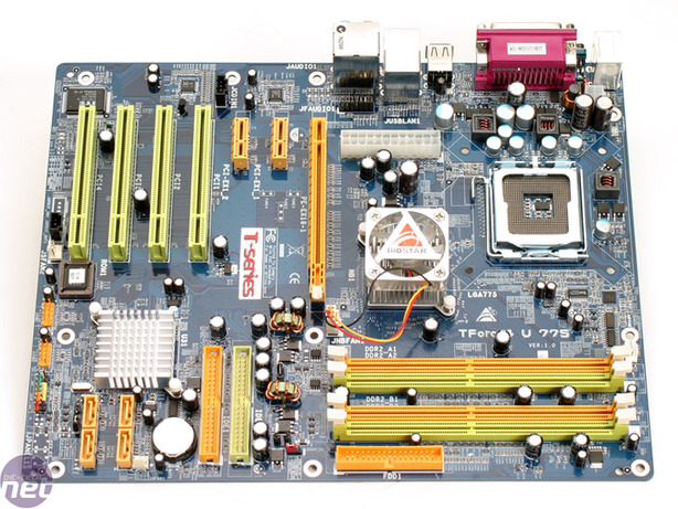
One such problem with the layout is the less-than-optimal positioning of the 24-pin ATX power connector, which is located right next to the back panel connectors for USB2.0 and audio. Cable routing would be much easier if this was positioned along side, or nearer to the floppy drive port located next to the memory slots.
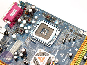
The area around the CPU socket is clear, but we found that the positioning of the 24-pin ATX power adapter could prove to be a problem if you're using a larger heatsink, like one of Zalman's CNPS9500-series coolers. The positioning means that the 24-pin ATX power cable will need routing across the motherboard and across components. The most obvious way to route the cable would be across the mosfets and capacitors next to the 4-pin ATX 12v connector.
The board uses a three-phase voltage regulator power design and this limited the board somewhat when overclocking. The board is targeted at the budget gaming enthusiast that is likely to overclock his system. With that in mind, along with the increasing power requirements on Intel's processors, it would have been good to see at least a four-phase power circuit implemented on this board.
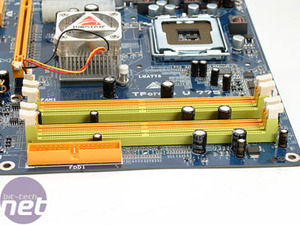
The memory slots are parallel to the bottom edge of the board with the floppy disk connector along side them. The DIMM slots are coloured by pairs of channels, rather than by channel. This means that it's easier to work out which memory slots you need to install your DDR2 memory into.
In between the memory slots and the two IDE connectors, there is a jumper labelled JDDR2_OV_3V. This is designed for use when overclocking the motherboard, however there are some limitations to its use. When the jumper is changed from the default position (with the jumper closed over Pin 2-3) to close Pin 1-2, the voltage is fixed to 3.3V automatically. There is no way to change this value in the CMOS and it strikes us as being a little bit crazy for DDR2 memory, considering its default voltage is a mere 1.8V.
We spoke to one of Corsair's lead engineers about this, and he confirmed our initial concerns. 3.3V is an insane amount of voltage to send through a DDR2 memory module. The module is likely to be damaged within hours at best case and instantly at worst case. It seems a little crazy to feed 3.3V through DDR2 memory modules and one would expect it to be a typo if it was only in the manual. However, the fact that the board also indicates that at least 3V is sent through the memory when you switch the jumper, we'd suggest leaving the jumper where it is unless you're planning on making toasted DDR2 sandwiches.


MSI MPG Velox 100R Chassis Review
October 14 2021 | 15:04


Want to comment? Please log in.