
With the cost of energy increasing almost by the day, the focus on energy efficiency in the technology industry is starting to become more and more prominent. With Intel seemingly back up to firing on all cylinders with its Core 2-based processors, AMD has been playing a game of catch up, because its K8 architecture is starting to show its age after over three years of service.
During the later stages of the Netburst era (since the day that AMD’s K8 launched), Intel’s advantages in process technology didn’t matter a great deal to AMD, because the underdog had a better performing and more power efficient architecture. The processor game was a pretty one-sided affair back then – at least, in the enthusiast space – but things changed quite dramatically in that incredibly busy month of July last year.
Not only did Intel launch its first Core 2 Duo processors with incredibly aggressive pricing, AMD cut the price of many of its CPUs in half overnight in order to react to Intel’s massive improvements in both performance and energy efficiency. Today we are looking at one of AMD’s first 65-nanometre ‘Brisbane’ processors, which were quietly announced back on the 5th December. Given the fact that Intel launched its first 65nm Cedar Mill and Presler-based (a pair of Cedar Mill’s on one CPU package) Pentium 4 and Pentium D processors on 27th December 2005, it shows the lead that Intel has when it comes to manufacturing technology.
Manufacturing technology isn’t everything though, as AMD has proven in the past, but with both David and Goliath having relatively good CPU architectures it can play an important part. Reducing the process node usually results in lower power consumption, lower operating voltages and thus, more modest cooling requirements.
While AMD hasn’t promised any notable changes in performance with the process shrink, we’ve put AMD’s new Athlon 64 X2 5000+ EE processor through its paces in our typical selection of benchmarks. Before we get to that though, let’s have a look at what’s new.
It’s a typical practice in the semiconductor industry for a manufacturer to shrink a familiar ASIC with finer manufacturing process technology before attempting to produce something completely new on the unknown process. This allows the semiconductor manufacturer to mature the process with a design that it is incredibly familiar with, taking most ASIC design related problems out of the equation.


AMD's Fab 36 in Dresden, GermanyAccording to AMD, the new 65nm G-stepping Brisbane core has the same transistor count as the 90nm F-stepping Windsor core (just shy of 154 million transistors in real terms) that it will eventually replace. As a result of the finer manufacturing process, the Athlon 64 X2 die has been reduced from 183mm² to 126mm² – just shy of 69% the size of its older brother. If my calculations are correct, a perfect die shrink from 90nm to 65nm would make the 65nm ASIC 52% of the size of the same ASIC manufactured on a 90nm process.
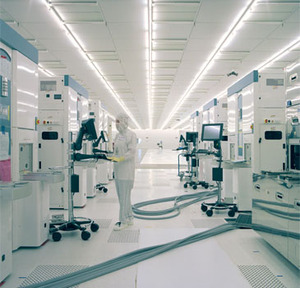
The reduction in die size obviously means that AMD is able to get more dies per wafer, however there’s more to it than meets the eye. The chips are manufactured at AMD’s Fab 36 manufacturing plant in Dresden, Germany. This plant exclusively uses 300mm wafers, while AMD’s Fab 30 facility (which is located right next to Fab 36) uses 200mm wafers that have less than half the surface area of a larger 300mm wafer (31,415mm² versus 70,685mm²).
Producing processors using a 300mm wafer is cheaper on a per die basis than producing the same processors on a 200mm wafer. If you take that and the impressive 31% die size reduction that AMD has managed to attain, the company’s cost of producing Athlon 64 X2 processors has just plummeted.
The lower production costs aren’t going to mean cheaper processors though, because the process shrink is designed to increase AMD’s margins and production capacity. This will enable the chip manufacturer to satisfy the demand for its processors, and increase production capacity in the future. I know that the selfish amongst you won’t like that fact because the process shrink is all about earning more money for AMD (rather than saving money for the consumer). As far as I’m concerned though, that’s good for the microprocessor industry – it’s important to have both AMD and Intel pushing technology forwards for the sake of healthy competition.
During the later stages of the Netburst era (since the day that AMD’s K8 launched), Intel’s advantages in process technology didn’t matter a great deal to AMD, because the underdog had a better performing and more power efficient architecture. The processor game was a pretty one-sided affair back then – at least, in the enthusiast space – but things changed quite dramatically in that incredibly busy month of July last year.
Not only did Intel launch its first Core 2 Duo processors with incredibly aggressive pricing, AMD cut the price of many of its CPUs in half overnight in order to react to Intel’s massive improvements in both performance and energy efficiency. Today we are looking at one of AMD’s first 65-nanometre ‘Brisbane’ processors, which were quietly announced back on the 5th December. Given the fact that Intel launched its first 65nm Cedar Mill and Presler-based (a pair of Cedar Mill’s on one CPU package) Pentium 4 and Pentium D processors on 27th December 2005, it shows the lead that Intel has when it comes to manufacturing technology.
Manufacturing technology isn’t everything though, as AMD has proven in the past, but with both David and Goliath having relatively good CPU architectures it can play an important part. Reducing the process node usually results in lower power consumption, lower operating voltages and thus, more modest cooling requirements.
While AMD hasn’t promised any notable changes in performance with the process shrink, we’ve put AMD’s new Athlon 64 X2 5000+ EE processor through its paces in our typical selection of benchmarks. Before we get to that though, let’s have a look at what’s new.
Let's all head to Brisbane...
Brisbane is quite an important CPU for AMD in many respects, because the company’s next-generation K8L processor is going to be manufactured on the same 65 nanometre Silicon On Insulator process. Between now and the time when AMD launches its native quad-core processor, AMD will work to make the process as mature as possible by the time the new architecture is ready to launch.It’s a typical practice in the semiconductor industry for a manufacturer to shrink a familiar ASIC with finer manufacturing process technology before attempting to produce something completely new on the unknown process. This allows the semiconductor manufacturer to mature the process with a design that it is incredibly familiar with, taking most ASIC design related problems out of the equation.
AMD's Fab 36 in Dresden, Germany
The reduction in die size obviously means that AMD is able to get more dies per wafer, however there’s more to it than meets the eye. The chips are manufactured at AMD’s Fab 36 manufacturing plant in Dresden, Germany. This plant exclusively uses 300mm wafers, while AMD’s Fab 30 facility (which is located right next to Fab 36) uses 200mm wafers that have less than half the surface area of a larger 300mm wafer (31,415mm² versus 70,685mm²).
Producing processors using a 300mm wafer is cheaper on a per die basis than producing the same processors on a 200mm wafer. If you take that and the impressive 31% die size reduction that AMD has managed to attain, the company’s cost of producing Athlon 64 X2 processors has just plummeted.
The lower production costs aren’t going to mean cheaper processors though, because the process shrink is designed to increase AMD’s margins and production capacity. This will enable the chip manufacturer to satisfy the demand for its processors, and increase production capacity in the future. I know that the selfish amongst you won’t like that fact because the process shrink is all about earning more money for AMD (rather than saving money for the consumer). As far as I’m concerned though, that’s good for the microprocessor industry – it’s important to have both AMD and Intel pushing technology forwards for the sake of healthy competition.
RELATED ARTICLES


MSI MPG Velox 100R Chassis Review
October 14 2021 | 15:04


Want to comment? Please log in.