
According to a report on DailyTech, there is more to AMD’s upcoming tri-core Phenom processors than you would have first thought – it's possible that not all of the tri-core processors will be merely cut-down versions of the existing quad-core ‘Agena’ chip used in the chip manufacturer’s first Phenom processors.
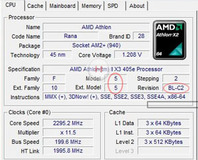
The first batch of the soon-to-be-released tri-core processors are codenamed ‘Toliman’ – these are based on the Agena die, meaning that the full 2MB of shared L3 cache intact, even though one the cores has been disabled.
These products will fit under the Phenom 8000 umbrella and, according to DailyTech, the first processors to be released will be the 2.4GHz Phenom 8700 and the 2.3GHz Phenom 8600. Anonymous AMD representatives said that both of these will launch with a 95W thermal envelope.
AMD’s first 45nm quad-core processors will be released at the end of 2008, and these will be followed in 2009 by dual- and tri-core processors. DailyTech says that AMD’s roadmap states that the 45nm quad-core processors will be DDR3-only; however, the triple-core ‘Heka’ processors will feature both DDR2 and DDR3 support.
Interestingly, both 45nm quad- and triple-core processors will be available in two variants – one with shared L3 cache, and one without. What’s not clear though is what ‘Heka’ actually is – is it a combination of the excess quad-core processors with (Deneb) and without (Propus) shared L3 cache, or is it a completely new die?
To make matters a little more unclear is another chip on AMD’s roadmap: ‘Regor’. DailyTech’s report says that ‘Regor’ is believed to be a dual-core version of ‘Deneb’, but it will apparently come with “variable shared L3 cache and a mix of DDR2 and DDR3 support.” It’s ultimately possible that this jungle of codenames actually results in just two different dies—‘Deneb’ and ‘Propus’—with ‘Heka’ and ‘Regor’ being variants of the two with one or two of the cores disabled.
Discuss in the forums.
RELATED ARTICLES


MSI MPG Velox 100R Chassis Review
October 14 2021 | 15:04


Want to comment? Please log in.