
It's nearly half the size...
The move to 90 nanometres has many gains, the biggest being the ability to shrink the die and reduce the cost of producing the GPUs. NVIDIA has managed this with G71, and it's possible for them to fabricate nearly twice as many cores on a wafer.The core is nearly half the size of G70 - it was roughly 334mm² in size, while G71 is a mere 196mm² by comparison. In contrast, ATI's R580 GPU - which is manufactured on TSMC's 90 nanometre low-k fab process - is 316mm²; that's over one and a half times the size. This comes down to the fact that they've included their ring bus memory controller - which takes up a massive amount of die space - we're told that it takes up around 80 million transistors, which equates to around 20% of the total die space.
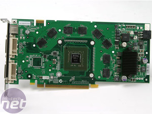
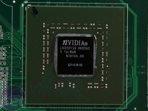
GeForce 7900 GTX & G71
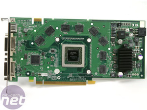
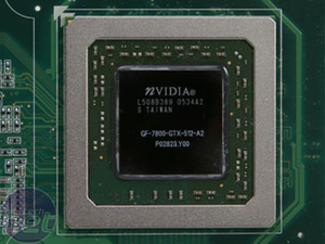
GeForce 7800 GTX 512 & G70
The biggest difference between the two is the lack of the Phillips SAA7115 video decoder chip that is midway between the GPU and the DVI ports to the rear of the card. This chip decodes PAL, NTSC and SECAM video input streams. NVIDIA decided not to use the chip on its GeForce 7900 GTX reference cards and partners seem to have followed suit too. They told us that most customers are opting to use other means for video-in including USB, Firewire and TV tuners. Of course, this doesn't stop partners from including the SAA7115 if they choose to, because the solder points are still present on the PCB.
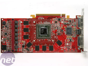
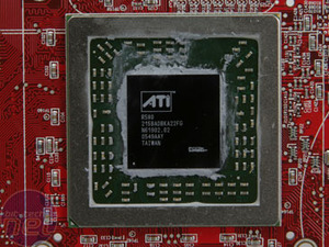
Radeon X1900XTX & R580
The performance differences aren't massive when running at the same clock speeds, but ATI's architecture seems to be more forward looking as it's geared more to running higher resolutions with lots of antialiasing enabled. NVIDIA didn't think that the die space was worth it at this moment in time and we're inclined to agree with that. At least, for the time being. When games start to make use of increasing amounts of memory more often, we might see some benefits from using eight 32-bit memory channels over NVIDIA's four 64-bit channels.


MSI MPG Velox 100R Chassis Review
October 14 2021 | 15:04


Want to comment? Please log in.